When a signal is applied at the input pin of a logic gate then the output doesn’t change instantly. It will take some time to reflect the effect of change from the input Signal to the output, this is termed as “Propagation Delay” or Propagation Delay is defined as the difference between 50% change in the input signal and 50 % change in the output signal. For example, Refer to Fig.1 where OR Gate is used. The Input A is fixed to 0 and B changes from 0->1 thus the output Y changes from 0->1 after some time which is referred to as Propagation Delay.

Fig. 1: Propagation Delay
How Gate Delay is Calculated
Propagation Delay depends on two factors:
- Input Transition
- Output Load Capacitance
Transition Delay/Slew
It is defined as the time taken to change the state of Signal from Low-High or High-Low. There are mainly two types of transition:
- Rise Transition
Rise Time is defined as the time it takes for a signal to reach from its 10% value to its 90% value
- Fall Transition
Fall Time is defined as the time it takes for a signal to reach from its 90% value to its 10% value.
- Rising Edge
In a positive edge triggered design the edge which is changing its value from logic 0 to logic 1 is known as rising edge.
- Falling Edge
In a positive edge triggered design the edge which is changing its value from logic 1 to logic 0 is known as falling edge.
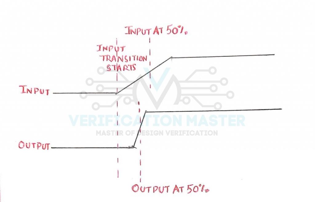
Fig.2 Rise Transition and Fall Transition
Propagation Delay is directly proportional to transition time when output load capacitance is kept constant. So, as the transition time increases which means the signal is switching slowly as a result Propagation Delay increases. To have less Propagation Delay Transition Time should be less which means the signal should switch faster.
Output Load Capacitance
Load Capacitance
It is the sum of the input capacitance of the circuit and the interconnect capacitance. When the length of the interconnect increases the load capacitance also increases. As the load capacitance increases, it demands more transient current at the output. Every output pin has a limited value of current capability. So, the increase in load capacitance results in slowing down the edges or increases delay.
Output Load Capacitance is the value of Capacitive Load that an Output Pin can Drive. If the Load Capacitance is exceeding the defined value then it will lead to violations because charging and discharging will be slow now. As the number of standard cells connected to the output pin increases the value of Capacitive Load increases.
Propagation Delay is directly proportional to Output Capacitive load when Transition Time kept constant. So, if there is a less Capacitive Load at the output pin, it will take less time to discharge thus Propagation Delay will be less and if the Capacitive Load is high it will take more time to discharge, and thus Propagation Delay will increase.
There are LUTs (lookup tables) in the Liberty File which gives the information of propagation delay of each standard cell. Lookup Tables are formed by interpolation and extrapolation of transition time vs load capacitance value. So, using the information present in Liberty File you can optimize the timing.
Interpolation
When a third value is estimated from a list of two known values.
Extrapolation
Approximation of third value by extending a known set of values.
Negative Propagation Delay
In general cases, the output changes only after the application of input. But, in few cases, the output changes faster than the input which gives rise to Negative Propagation Delay. It is possible in the below cases:
- Transistor with High Drive Strength
- Slow Input Transition
- Small Load at Output
Under the above-mentioned conditions out will switch faster than input giving rise to negative propagation delay.
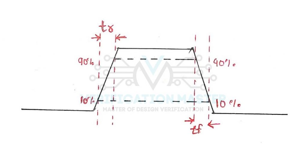
Fig.3 Negative Propagation Delay
So, from this blog you can answer the below set of questions:
-
- Q1) What is Propagation Delay?
- Q2) What is Transition Time or Slew?
- Q3) What is Load Capacitance?
- Q4) How Propagation Delay depends on Transition Time and Output Load Capacitance?
- Q5) Give waveform to explain Propagation Delay,
- Q6) What is Negative Propagation Delay?