Net Delay
The difference in time taken by a signal when it is applied at one end of a net and reaches the other components connected to another end of the net is referred to as Net Delay. Net Delay is present due to the resistance and capacitance of the net and it is also known as Wire Delay
Net Parasites
In SoCs, metal layers are used for interconnect. The number of metal layers available is based upon the technology node of SoC. VIAs are present to connect one metal layer to the other metal layer. Between two metal layers, a dielectric material is present. The metal layers used should follow a few design rules in which the two most important are minimum metal layer width and the second one is the minimum spacing between two metal layers. Before the fabrication process, the layout must specify the design rules to ensure proper manufacturing of SoC. As per the technology node the metal width, spacing, and thickness of metal layers vary. With the decrease in the technology node width, spacing and thickness value decreases.
Metal Layers or interconnects introduce two very important factors in the design that should be taken care of and these are resistance and capacitance. Resistance and capacitance combined form Net Parasitics.
Interconnect Resistance
Every metal has a property called resistivity. Resistivity can be defined as the obstruction caused to the flow of current in a circuit. Based on the metal properties, resistivity varies. Insulators have very high resistivity, semiconductors have moderate resistivity, and conductors have low resistivity.
The mathematical formula for resistance = Resistivity/(Width of metal layer)*(Thickness of metal layer)
With the decrease in the technology node width and thickness of the metal layer also decreases. So, Resistance increases with decreasing technology.
As the Delay of the signal is directly proportional to the resistance, that’s why the design team always tries to have minimum resistance in the circuit. Previously in higher technologies, Aluminum was used for interconnects but, in lower technology nodes copper is used as interconnects. The reason behind shifting from aluminum to copper is that copper has 2 times lower resistance as compared to aluminum. So, the speed of SoC is improved.
The resistivity of a material varies with temperature. Below is the relation:
ρ = ρ0(1 + α(T − T0))
where α is the temperature coefficient of resistivity, T0 is the room temperature and ρ0 is the resistivity at room temperature.
In intrinsic semiconductors, the resistivity decreases with increasing temperature. The electrons can move from valence band to conduction band by application of thermal energy. In a typical non-doped intrinsic semiconductor the resistivity decreases exponentially with temperature.
But, interconnects are made of Aluminum or copper both are metals/conductors. So, T↑ R↑, W↓ R↑ and T↓ R↑
Interconnect Capacitance
In a design, the routing of interconnecting wires is very close to each other, due to this charges are stored in wires. So, when a signal is traveling through these interconnect wires the wires act like a charged plate. The possible scenarios are :
- The neighboring wire contains some amount of charge.
- No signal i.e. acts like a grounded wire.
- Same signal flowing at the same time.
The last case is rare. According to the first and second cases a capacitance may or may not be present.
Interconnect capacitance can be differentiated according to the interaction of conductors/plates with each other.
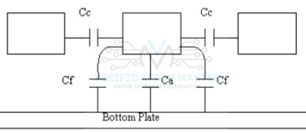
Fig. 1: Type of Capacitance
Refer to above figure there can be three types of capacitance
- Coupling Capacitance (Cc)
- Area Capacitance (Ca)
- Fringe Capacitance (Cf)
Cbottom = Ca + 2Cf
Csum = Ca + 2Cf = 2Cc
Ctotal = Total Capacitance of the central wire
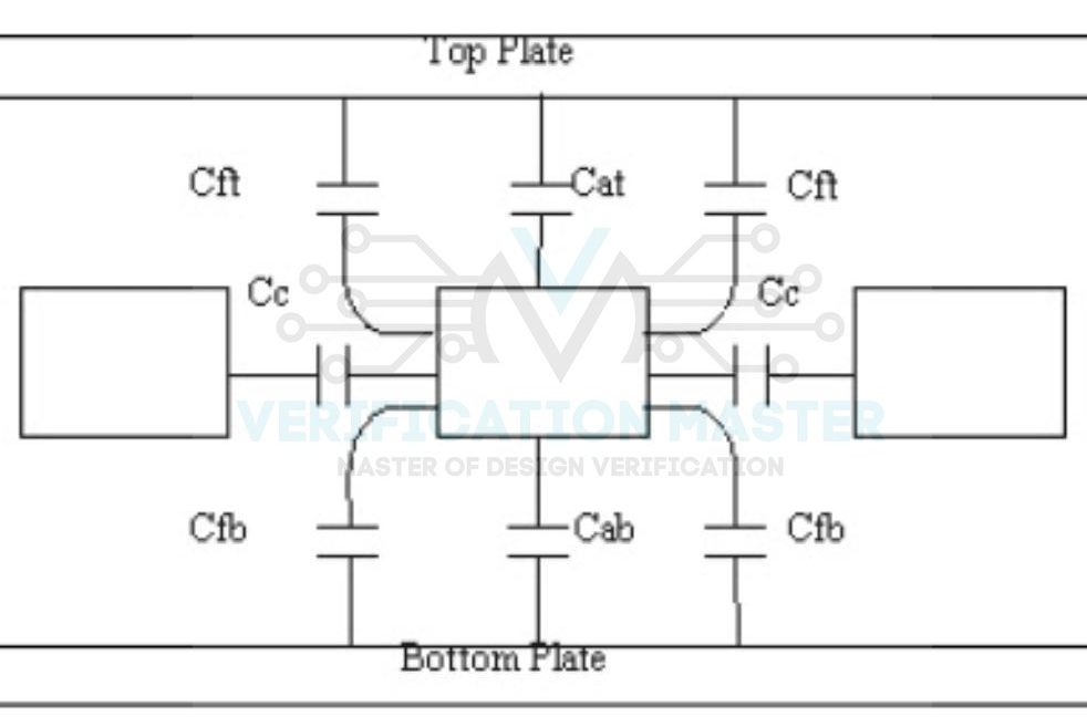
Fig. 2: Middle Capcitance
Refer to the above figure the capacitance are:
Cc – Coupling Capacitance, Cat – Area capacitance with the top portion, Cab – Area Capacitance with the bottom portion,
Cft – Fringe Capacitance wrt top ground surface, Cfb – Fringe Capacitance wrt bottom ground surface.
Ctop = Cat + 2Cft
Cbottom = Cab + 2Cfb
Csum = (Cat + 2Cft) + (Cab + 2Cfb) + 2Cc
Ctotal = Total Capacitance of middle central wire
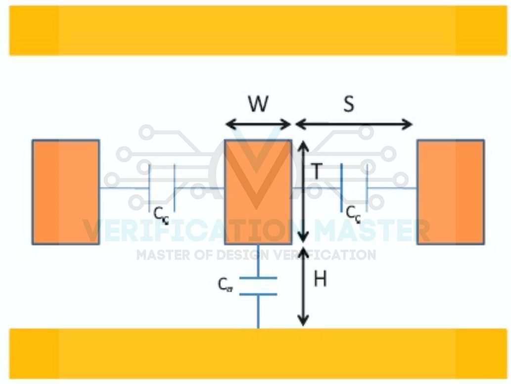
Fig. 3: Surface Capacitance Per Unit Length
Refer to above figure. The formula for surface capacitance per unit length = ε*(metal width)/(dielectric thickness) = ε*W/H
The formula for coupling capacitance per unit length = ε*(metal thickness)/(spacing between metal wires) = ε*T/S
So, for capacitance, we can conclude that
- W↓ –> Ca↓
- S↓ –> Cc↑
- T ↓ –> Cc↓
But, with the decrease in the technology size the rate by which the thickness of metal decreases in comparison to the space between them is less. So, down the technology the coupling capacitance increases. So, in lower technology Designers focus more on Crosstalk and Signal integrity which occurs due to coupling capacitance.
From this blog you can answer the below set of questions:
- Q1) What are net parasitics?
- Q2) Explain Resistance in interconnect wires.
- Q3) Explain Capacitance in interconnect wires.