Generated Clock
When a clock is derived from a master clock it is referred to as a generated clock. The master clock is a clock defined by using the create_clock command.
For example, if the generated clock is divided by 4 of the master clock, then the generated clock is defined in the output of the circuit. It is important to specify the generated clock as STA has no information about the change in the clock period at the output of the divide-by logic. The generated clock is also a part of the design.
Example:
create_clock -name CLKP 10 [get_pins UPLLO/CLKOUT]
This command will create a master clock with name CLKP of 10ns period with 50%duty cycle at CLKOUT pin of PLL
create_generated_clock -name CLKPDIV2 -source UPLLO/CLKOUT -divide_by 2 [get_pins UFFO/Q]
This command will create a generated clock with the name CLKPDIV2 at the Q pin of the flip-flop UFFO. The master clock is CLKP and the period of the generated clock is double of master clock i.e. 20 ns.
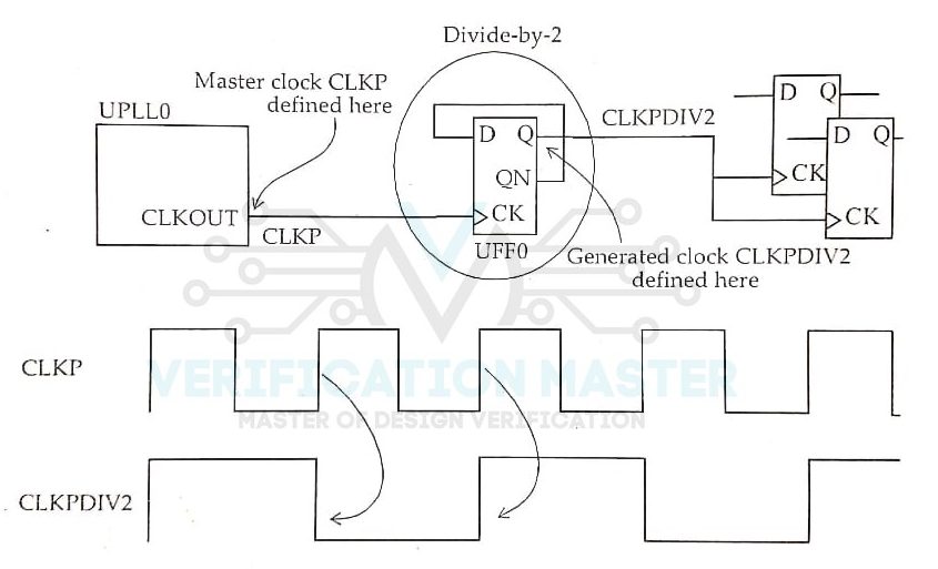
Fig. 1: Master Clock and Generated Clock
The above Fig.1 shows the circuitry and waveform for the master clock and the generated clock.
Now, a question may arise that can we define a new clock i.e. a master clock at the flip-flop output instead of a generated clock?
The answer is Yes, we can do this. But, doing this will create a new clock domain. So, this can create a problem if there are more clock domains already present in the design to deal with. The generated clock does not create a new clock domain. And also generated clock is in phase with the master clock.
The origin of the master clock is the point of definition of the master clock and the origin of the generated clock is that of the master clock. So, in the timing report, the start point is always the definition point of the master clock. It has an advantage of a generated clock over defining a new master clock as the source latency is not automatically included in the case of the new master clock.
Clock Generation Scenarios
Refer to Fig.2 which shows clock distribution in an ASIC. The oscillator that produces a clock with low frequency (10-50MHz) is external to the ASIC chip and it is used as a reference clock by on-chip PLL for generating a high-frequency clock (200=800 Mhz). The clock divider used the PLL clock to generate the required clock for the ASIC.
There are clock gates present on some of the branches of clock distribution. Clock gates turn off the clock during the inactive part of the design which helps in saving power whenever required. A multiplexer at the PLL output helps in PLL bypass whenever necessary.
There are two master clocks, one master clock is at the input pin of the chip and the second master clock is defined at the PLL output. Clocks that are generated by the clock divider are referred to as generated clocks.
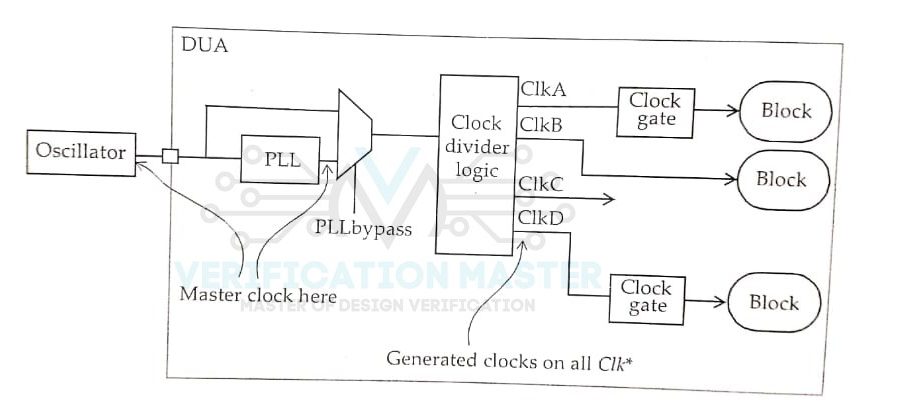
Fig. 2: Clock Distribution in ASIC
Virtual Clock
A clock that is not connected to any pin or port logically to the Design and also doesn’t exist physically in the Design is known as a virtual clock. In STA it is used for specifying the input and output delays signal coming from or going to a block that does not contain any clock.
A virtual clock is introduced in the design only during the timing optimization Virtual Clock do not have any actual clock source. Refer to Fig.3 where the design is getting clock from CLK_CORE, but clock driving input port ROW_IN is CLK_SAD. Similarly, this problem is present for output port STATE_O.
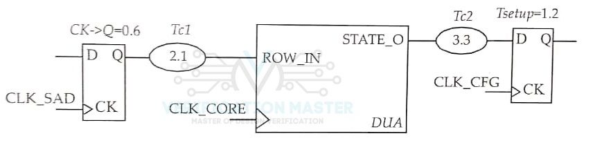
Fig. 3: Virtual Clock
To solve such problems virtual clock is introduced with no information about the source pin or port. In the above Fig.3 virtual clock is defined for CLK_SAD and CLK_CFG.
create_clock -name VIRTUAL_CLK_SAD -period 10 -waveform {2 8}
create_clock -name VIRTUAL_CLK_CFG -period 8 -waveform {0 4}
create_clock --period 10 [get_ports CLK_CORE]
After defining the above virtual clocks, the IO constraints can be defined in relation to the virtual clock as below:
set_input_delay -clock VIRTUAL_CLK_SAD -max 2.7 [get_ports ROW_IN]
set_output_delay -clock VIRTUAL_CLK_CFG -max 4.5 [get_ports STATE_o]
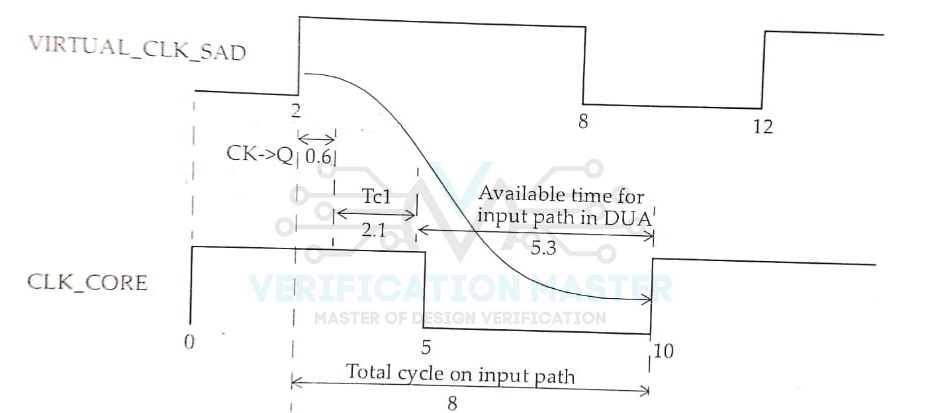
Fig. 4: Timing relationship on Input Path
Above Fig.4 represents the timing relationship on the input path. The input path of design under analysis is constrained to 5.3 ns or less.
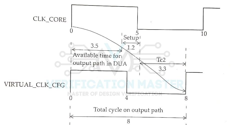
Fig. 5: Timing Relationship on Output Path
Above Fig.5 represents the relationship on the output path. The output path of the design under analysis is constrained to 3.5 ns or less.
The -min option with set_input_delay and set_output_delay is used for verifying the fast (min) paths in the design. Using a virtual clock is just one of the methods to constrain the inputs and outputs.
So from this blog, you can answer the below set of questions:
- Q1) What is the generated clock?
- Q2) Write the SDC command to define the generated clock.
- Q3) What is a virtual clock?
- Q4) Write the SDC command to define a virtual clock.