Multiple Clocks
When there are many clocks present in a design then they must be having different waveforms and frequencies. So, such clocks are referred to as multiple clocks, and the logic triggered by each clock is called clock domain. When clocks have different frequencies then they repeat over a common base period.
Asynchronous Clocks
When a design has multiple clock domains and there is no common base period for the different clocks, then it is referred to as Asynchronous Clocks. For example, clocks generated from different PLLs are Asynchronous clocks.
With the decrease in the Technology Nodes the Power Dissipation increases. So, to maintain a good PPA (Power Performance Area) strategy Power Dissipation must be controlled and should be taken into importance for a Design. One of the factors for Power Dissipation is the Frequent Switching Activity of the Signals in the Design that leads to Dynamic Power Dissipation. As in a Design Clock Elements like Buffers and few other Logic Gates that help in the propagation of Clock Signals, switches most frequently. So, they will contribute to a huge amount of Dynamic Power Dissipation for Design. So, to reduce the Power Dissipation due to the frequent Switching of the Clock Signals Clock Gating method is used.
The clock Gating method stops the clock for those elements in the Design whose Data is not toggling. Let’s take an example of a Flip-Flop which Toggles its Output only when the Enable is 1. So, as long as Enable = 0 the Output will not Toggle and the Clock Cycles will get wasted during this time and Power Dissipation takes place. To prevent the wastage of Clock cycles as long as Enable is 0 Clock Gating is implemented that stops the Switching of Clock signals when Enable is 0 and reduces Power Dissipation.
Clock Gating can be implemented using below two methods :
- Latch Free Clock Gating
- Latch Based Clock Gating
Latch Free Clock Gating
In this method, an AND or Or Gate is used. The Gate used depends on Triggering Edge of Flip-Flop. But one disadvantage of using Latch Free Clock Gating is that if Enable Signal goes down in between an Active Clock Pulses it will produce Glitches in the Gated Clock Cycles that can lead to improper functioning of the Design. To overcome this problem Latch based Clock gating is used.
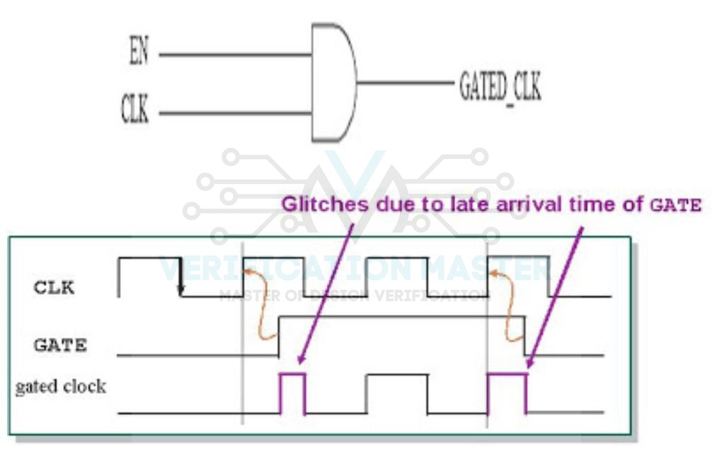
Fig 1 Latch Free Clock Gating
Latch Based Clock Gating
In this method, a Level Sensitive Latch is used before an AND Gate which will Hold the Enable Signal between the Active Edge and Inactive Edge of the Clock. State of the Enable signal is Captured by Latch and a proper and complete Clock Pulse is generated. The Enable signal needs to be secure around the Active Edge of the Clock.
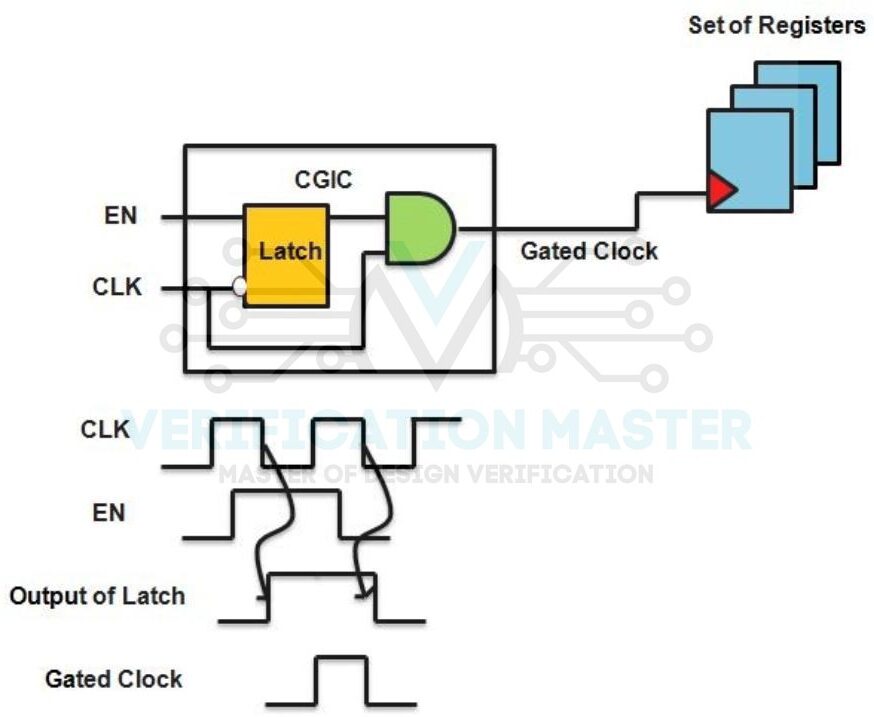
Fig 2 Latch Based Clock gating
So from this Blog, you can answer the below set of Questions:
- What is a Multiple Clock?
- What is an Asynchronous Clock?
- What is Clock Gating?
- Explain Latch Free Clock Gating.
- Explain Latch-Based Clock Gating.