In this blog, we will look at a subtopic known as Field Programmable Gate Arrays, or simply FPGA and CPLD.
We will discuss the principle of Programmable Logic Devices (PLD) and several of their types. We will also look at the architecture of a typical FPGA device and CPLD and its benefits.
Introduction
FPGAs are digital ICs (integrated circuits) that allow the hardware design engineer to create personalised digital logic based on his or her needs.
The name “Field Programmable” suggests that the IC’s Digital Logic is programmable by the end-user rather than being fixed during manufacture (or fabrication) (designer).
An FPGA is made up of programmable logic blocks and configurable interconnects to offer this programmability.
FPGAs’ programmable logic and interconnections (routing) make them general-purpose and adaptable, but they are also sluggish and power-demanding when compared to a comparable quality ASIC using Standard Cells.
Before moving into the main topic, we will quickly go over the concept of programmable logic devices. So, we will see exactly what we mean by the PLD.
PLD (Programmable Logic Device)
It is an integrated circuit (IC) that has a huge number of logic gates and flip-flops that may be set by the user to perform a wide range of operations.
The most basic programmable logic device is an array of AND & OR gates, and the logic of these gates and their interconnections may be programmed.
When a developer wants to develop customised logic but is limited by pre-configured integrated circuits, PLDs are beneficial.
PLDs enable the implementation of a customised digital circuit by utilising the power of hardware configuration rather than software.
Types of PLD
The Simple Programmable Logic Devices are further classified as follows:
- Programmable Logic Array (PLA)
- Programmable Array Logic (PAL)
- Generic Array Logic (GAL)
PLDs are broadly classified into three categories. They are as follows:
- Simple Programmable Logic Devices (SPLD)
- Complex Programmable Logic Devices (CPLD)
- Field Programmable Gate Arrays (FPGA)
Simple Programmable Logic Devices
We will discuss the simple PLD in a very short manner with the help of some figures and then move to our main topics, i.e., FPGA and CPLD.
Programmable Logic Array (PLA)
A PLA comprises an AND gate plane with programmable interconnects and an OR gate plane with programmable interconnects. A basic four-input-four-output PLA with AND and OR gates is shown in Figure 1.
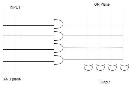
Fig 1: Programmable Logic Array (PLA)
Programmable Array Logic (PAL)
As we can see in figure 2, a PAL is identical to a PLA, however the AND gate plane in PAL is programmable whereas the OR gate plane is fixed after manufacturing. PALs are less versatile than PLAs, but they do not have the temporal delays associated with programmable OR Gates.
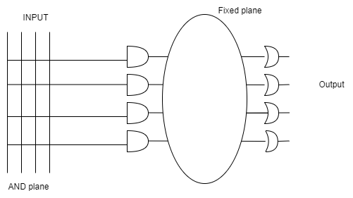
Fig 2: Programmable Array Logic
Generic Array Logic (GAL)
A GAL is architecturally identical to a PAL, but the distinction is in the programmable structure. PALs employ PROM, which is only once programmable, whereas GAL employs EEPROM, which can be reprogrammed.
So let’s move to the main topic, i.e., FPGA
Field Programmable Gate Arrays (FPGA)
FPGA is an abbreviation for Field-programmable Gate Array. An FPGA is, at its heart, a collection of linked digital sub-circuits that execute common operations while also providing extremely high degrees of flexibility.
FPGAs are semiconductor devices that are built around a matrix of customizable logic blocks (CLBs) coupled via programmable interconnects. After production, FPGAs can be reprogrammed to meet specific application or feature needs.
This characteristic separates FPGAs from application-specific integrated circuits (ASICs), which are designed specifically for specific purposes.
Although one-time programmable (OTP) FPGAs are available, the majority of FPGAs are SRAM-based and may be reprogrammed as the design changes.
In a general sense, the figure 3 below depicts the typical internal structure of an FPGA.
As you can see, the FPGA’s core consists of adjustable logic cells and programmable interconnections. These are surrounded by a number of programmable IO blocks that are used to communicate with the outside world.
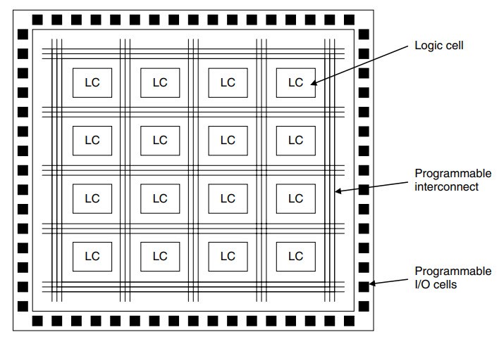
Fig 3: Field Programmable Gate Arrays
[Reference : FPGA | Field Programmable Gate Array | Introduction, Structure (electronicshub.org)]
Components
Let us now examine the construction of an FPGA in further detail. An FPGA is typically made up of three main components. They are as follows:
- Programmable Logic Cells (or Logic Blocks) are in charge of carrying out the essential logic functions.
- Programmable Routing is in charge of linking the Logic Blocks.
- The Input Output blocks are connected to the logic blocks via routing and assist in making external connections.
Technologies
We’ve discussed a lot about FPGAs’ reprogrammable design, but now let’s look at some of the most often utilised programming approaches that are responsible for such reconfigurable architecture.
The three well-known programming technologies utilised in FPGAs are as follows:
- SRAM:
We already know that there are two forms of semiconductor RAM: SRAM and DRAM. SRAM stands for Static RAM, whereas DRAM stands for Dynamic RAM.
SRAM is built with transistors, and the name “static” refers to the fact that the value stored on a basic SRAM Memory Cell will remain constant until it is modified or the power is withdrawn.
- EEPROM / Flash:
EEPROM or Flash programming technologies are a near substitute for SRAM-based programming technology.
The major benefit of flash-based programming is that it is non-volatile. Although flash allows for reprogramming, the number of times this can be done is highly limited when compared to SRAM technology.
- Anti-Fuse:
The anti-fuse programming technology is an ancient method of generating one-time programmable devices. They are implemented using an anti-fuse, which has a very high resistance in its un-programmed condition and can be regarded as an open circuit.
Applications
FPGAs are used in many fields in many ways. Let’s discuss that.
- FPGAs were first utilised to create small-to-medium complicated state machines and data processing operations on tiny data sets.
- FPGAs were a simple choice for prototyping ASIC designs since they could be quickly altered to test and try numerous versions of the hardware before finishing the primary design.
- Modern FPGAs with multipliers, complicated routing, and on-chip RAM can permit DSP tasks that were previously only achievable on specialist digital signal processors.
- FPGAs are becoming major rivals for embedded control applications as their costs fall. An FPGA may be used to build any microcontroller’s soft-core CPU as well as specialised I/O features.
Complex Programmable Logic Devices (CPLDs)
Complex Programmable Logic Devices (CPLDs) are just what their name implies. They are essentially meant to look like a huge number of PALs on a single chip, linked to one another through a cross-point switch.
They employ the same development tools and programmers and are built on the same technology, but they can handle far more complicated logic and a greater amount of it.
Architectures
The internal design of a typical CPLD is seen in Figure4. While each manufacturer has a unique version, they all include function blocks, an input/output block, and an interconnect matrix in common.
The devices are programmed using programmable elements, which might be EPROM cells, EEPROM cells, or Flash EPROM cells, depending on the manufacturer’s technology.
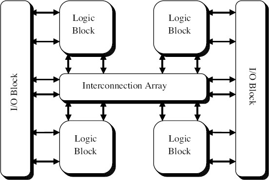
Fig 4: CPLD architectures
[Reference: https://www.researchgate.net/figure/A-simplified-block-diagram-of-CPLD-architecture-4_fig54_318725875]
Functional Blocks
The I/O blocks, other function blocks, or feedback from the same function block can all be sent through the AND plane.
The elements are then ORed together with a set number of OR gates before being picked by a big multiplexer. The mux outputs can then be transmitted directly out of the block or via a timed flip-flop.
This block offers extra logic such as a selectable exclusive OR and a master reset signal, as well as the ability to programme the polarity at various stages.
I/O Blocks
The I/O block is used to send signals to the CPLD device’s pins at the proper voltage and current levels. A flip-flop is usually supplied.
This is done on outputs so that timed signals can be delivered straight to the pins without being delayed.
It is done for inputs to reduce signal latency before reaching a flip-flop, which would increase the device hold time required.
Interconnect
The CPLD interconnect is a massive programmable switch matrix that allows signals to go from one portion of the device to another.
While no switch can link all internal function blocks to all other internal function blocks, there is enough flexibility to allow for many different connections.
So we learned the fundamentals of FPGA and CPLD from this blog. So let’s summarise the whole blog in a few questions so that it will be clearer.
- What exactly do you mean by FPGA?
- What is CPLD actually?
- What exactly do you mean by PLD?
- What is a simple PLD and what types are there?
- Please clarify how you categorise the PLD.
- What are the FPGA components?
- Explain the CPLD architecture.