We studied gate-level modelling in a previous blog and from there we can summarise that digital elements are binary things that can only have one of two values: 0 or 1.
The transitions from 0 to 1 and 1 to 0 include a transitional delay, as does each gate element in order to transfer the value from input to output.
For example, a two-input AND gate must flip the output to 1 if both inputs become 1 and return to 0 if any of its inputs becomes 0. When instantiating logic in Verilog, these gate and pin-to-pin delays can be defined.
There are three types of delays.
Rise Delay
A rise delay is the duration of time it takes for a gate’s output to shift from some value to 1.
Fall delay
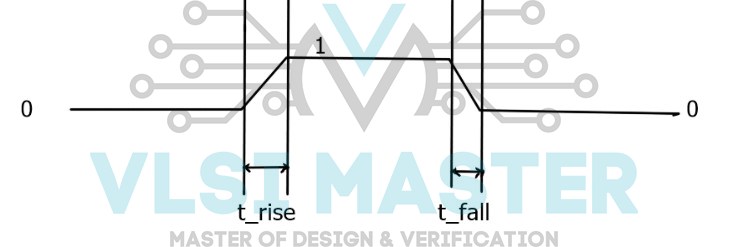
Fig 1: Rise and Fall Delay
A fall delay is the duration of time it takes for a gate’s output to go from some value to 0.
Turn-off Delays
Turn-off delay refers to the time it takes for the output of a gate to transition from some value to high impedance.
Such delays are relevant to every signal since they may all rise and fall at any moment in practical circuits and are not limited to gate outputs. There are three ways to express gate delays, and the first two are applicable to most primitives whose outputs do not transition to high impedance.
It will be very clear to you if you read the syntax of these delays.
- // Rise, Fall, and Turn-off Delay specification
- bufif0 #(rise_val, fall_val, turnoff_val) b1 (out, in, control);
Examples
Consider a basic example to demonstrate how gate delays may be used to simulate time in logic circuits. The following logic equations are implemented using an AND gate having a delay of 5 time unit.
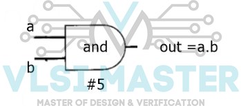
Fig 2 AND gate with a 5 time unit delay.
Verilog of above shown figure 2 is:
module des (input a, b, output out1);
// AND gate has 5 time unit gate delay
     and #(5) o1 (out1, a, b);
endmodule
module tb;
  reg a, b;
 wire out1;
  des d0 (.out1(out1),.a(a), .b(b));
  initial begin
{a, b} <= 0;
    $monitor ("T=%0t a=%0b b=%0b and=%0b ", $time, a, b, out1);
    #10 a <= 1;
    #10 b <= 1;
    #10 a <= 0;
    #10 b <= 0;
 end
endmodule
And the output of this blog is:
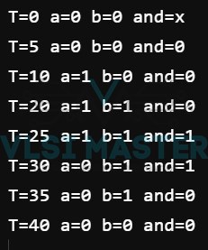
Fig 3: Output
As we execute this code, we can easily observe that the output is getting a delay of 5 time units. At time 20, both inputs are 1, and the output should be 0, but it is 1 due to a 5 unit delay; however, we can see the desired output at t = 25 and so on.
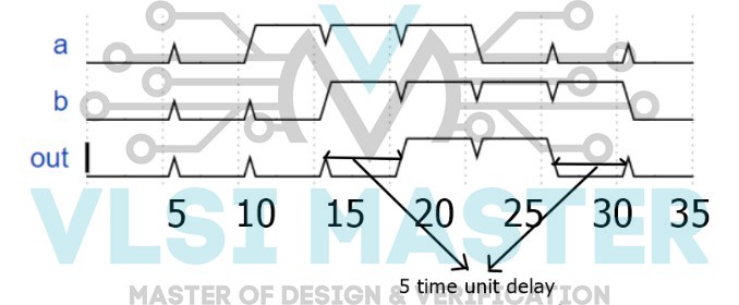
Fig 4: Timing Waveform
Figure 4 shows the timing waveform of Figure 2. It will give a clearer concept of the delay.
Min/Typ/Max Delays
Delays differ in different parts of the fabricated chip, as well as in different temperatures and other variations. As a result, Verilog provides an additional level of control for each of the delay types mentioned above. Every digital gate and transistor cell has a minimum, typical, and maximum delay specified by process node, which is typically provided by fabrication foundry libraries.
For each type of delay-rise, fall, and turn-off-three values can be specified: min, typ, and max, which stand for minimum, typical, and maximum delays.
Let us understand this with an example.
module des ( input a, b, output out1, output out2);
and #(2:3:4, 3:4:5) o1 (out1, a, b);
bufif0 #(5:6:7, 6:7:8, 7:8:9) b1(out2, a,b);
endmodule
The output of the given example is shown in figure 3.
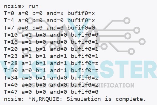
Fig 3 Min/Typ/Max Delays example
Hence, now we will summaries today’s blog. Let us see some of the questions that we can answer easily after reading this blog:
- What do you mean by the term “gate delays”?
- What are the types of gate delay?
- What is the difference between a rise delay and a fall delay?
- What is a turn-off delay?
- Write down the syntax of all the delays in and gates.