Tasks performed in the Routing Stage
- Global Routing
- Track Assignment
- Detail Routing
Global Routing
Before routing of traces is finalized, the implementation tool uses an estimate of routing distance to obtain RC parasitics of that route. Since routing is not yet finalized, the phase is called the global route. The estimated routes are used to determine resistance and capacitance(R &C). Using this estimated R &C wire delay is calculated. During this stage, one cannot include the effect of coupling. Only after the detailed routing is completed, actual R&C values are obtained and the effect of coupling can be analyzed.
This shows the overall connections between all the blocks in the design and the nets. The main aim for global routing is to minimize the total interconnect length and simultaneously reducing the critical path delay. This global routing step will determine the track assignments for each interconnect.
The Chip is completely divided into small blocks. These blocks are named as G-Cells. The size of the G-Cell will be based on the algorithm the tool uses. Each G-Cell will be having a finite number of horizontal and vertical tracks. Global routing will assign nets to specific G-Cells but it will not define a particular/specific track for each of them. The global router will connect two different G-Cells from a center point of each cell.
Track assignment
The global router will now assign tracks for all the interconnects in the design. The number of routing tracks available is dependent on the design and if die size is more, the higher the router tracks availability. Rach routing track has minimum width and minimum spacing distance. The value will be dependent on the technology used to build the design. If the routing demand goes over the availability, it causes congestion. Congestion simultaneously leads to DRC Errors and Slow runtime.
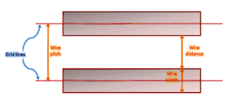
Metal Tracks
Grid lines can also be called as tracks.
Detailed Routing
In this step, the actual connection between all nets will take place. It creates the actual via, metal connections.
Aim of Detailed Routing
To minimize the total area, wire length, delay in critical paths.
Each layer posses specific tracks for interconnection, having its routing grid, rules. After detailed routing, the exact length and width of the metals/interconnects are known. Now the parasitic capacitance, resistance is extracted to determine the actual delays in the design. This is done by using extraction tools. The timing of the design is calculated based on the actual R & C Values by using Static Timing Analysis Tools. After timing is met, and all other verification is performed such as LVS, DRC, DFM (steps performed by Physical Verification Team) design is sent to the foundry to manufacture the chip.