What is ECO(Engineering Change Order)?
This process is performed when there is,
- Some functionality enhancement of the existing device. This functionality enhancement change might be very small to undergo all the process steps again.
- There might be some design bug that needs to be fixed which was caught very late in the design cycle. As it is very costly to re-run all the process cycle steps for each bug in terms of time and cost, some changes are to be taken incrementally.
Normally, there is a case that design enhancements/functional bug fixes are being implemented after the design has already been sent for fabrication. If suppose, the functional bug may be caught in the silicon itself. To fix the bug, it is not practically possible to restart the cycle.
The ECO process starts with the changes in the RTL code. The resulted netlist synthesized from the modified netlist is, then, compared with the golden netlist being implemented. The netlist, then, undergoes placement based on the incremental logic, clock tree modifications, and routing optimizations based upon the requirements.
What is IR Drop?
IR Drop is the voltage drop in the metal wires constituting the power grid before it reaches the Vdd pin of a standard Cells. Dynamic IR Drop is due to the switching of standard cells in the design. Higher switching leads to higher demand for current from the power supply.
What is Latch-up?
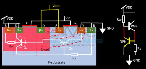
Latch-up is defined as a formation of a direct path from VDD to GND terminal in the design, which will cause a huge current flow between the power and ground terminal.
Inside a CMOS circuit, two parasitic BJT (Bipolar Junction Transistors) get formed and connected in such a way that these BJT form an SCR (Silicon-Controlled Rectifier) or Thyristor or PNPN device.
A pMOS device is formed inside a nwell and an nMOS device is formed in the p-substrate region. A parasitic PNP BJT formed here, whose emitter is the source of the pMOS, the base is the nwell and the collector is p-substrate. Similarly, a parasitic NPN BJT is formed near the nMOS device, whose emitter is the source of nMOS, the base is the p-substrate and the collector is nwell.
Both BJT’s are connected in such a way that they form a PNPN device. The base of PNP BJT is connected to the collector of NPN BJT and the base of NPN BJT is connected to the collector of NPN BJT.
Latch Formation
Normally PNPN device is in an OFF state and there is minimal current or no current flow through it. But once when it gets triggered by the gate signal, a large current starts flowing through it and continues to flow even if the gate signal is removed.
In short,latch-up is the phenomenon of activating the parasitic BJTs in a CMOS circuit which forms a low impedance path between the power and ground terminals. This low impedance path draws a large current and heats the IC (Integrated Chip) which causes permanent damage to IC.
How Latch-up is Triggered?
When the output voltage(Vout) has gone beyond the VDD due to noise, then it will forward bias the transistor between the drain terminal and nwell of pMOS. Once this junction is forward bias, the P+ region will start injecting hole to nwell. Now, these holes are collected by body contact of nMOS since it is connected to GND. So this event will start the movement of current from the drain of pMOS to the body of nMOS. Due to the flow of current, there will be a voltage drop between the source terminal of nMOS and the substrate below it. This now will aid for the forward bias of PN junction between substrate and source of nMOS. This eventually again starts injecting electrons from the N+ source to the substrate, which will be collected by the body terminal of pMOS which is connected to the VDD. So a loop/chain is formed and the next source terminal of pMOS and nwell will be forward bias. In this way, both the BJT has turned on and latched up.
Similarly, if output Voltage(Vout) goes below the VDD, the junction between the drain of nMOS and substrate will be forward bias, and this will make the junction between the source of pMOS and nwell forward bias and this will further again make the junction between the source of nMOS and substrate forward bias and both the BJT will be turned on and latch-up event occur.
When once the latch-up occurs in the CMOS design, lots of current start flowing directly from VDD to GND and will cause the failure of the chip. So to protect the chip from latch-up, Well-taps are used.
Well-taps are placed in parallel fashion in the design at a particular distance(depending on technology). This parallel fashion of connection makes the resistance reduce to R/x value and aids to drain the amplifying current flow (excess current which is damaging IC).
For Example: When three Taps are connected parallelly, Reff=R/3; where the R-value is reduced down to 3 units. As we know reduced R will maximize the current flow to get drained. Hence the amplified current gets a maximum chance to get drained and become nullified.
What are don’t use cells?
“Don’t use cells” are those cells which are present in the Library and you don’t want to use those cells in your design.
More in detail:
Whenever optimization is performed, then one has to provide a technology library. During mapping different logic of the design with proper cell or optimization of the design, the tool uses different types of cells (standard cell/ buffer/invertor/delay cell/filler cell), etc, present in the library. Since this Library is usually designed independently, so there are a lot of cells that are not required for a particular design.
Now, when there is no use of any particular cells because of any reason (like – driving strength, fanout, size, or design has some specific requirement or may be some type of cells are creating problem in your design during timing closer, etc) then one can mark or set an attribute over those cells in the design as don’t use cell. Now those cells will not be used in the design. Till the point they are used in a design, these cells are like Don’t use cell.
Some times designer set few cells as don’t use cells for some part of the design and then remove those attribute later on.
In short, Don’t use cells are not the type of particular cells but these are the attributes sets on the cells and for EDA tools. So they become don’t use cells.