Few of the objectives have to be maintained to achieve proper placement of cells in the design without degrading their functionality.
Performance(Timing):
In the placement stage, we only have placement of cells information but not their connectivity information. Routing is done in a way that it does not take much time for signal transition giving reasonable results wrt to the cell placement we did in this stage. This is called as Trail Route.
Early Global Route(Trail Route)
- A fast signal router is needed for the extraction of RC values and timing analysis.
- Used for congestion analysis
- This is not DRC/LVS clean. Trail route quickly routes design without fixing DRC/LVS.
Steps for Timing Analysis
- Look for the Quality of Report(QOR) or Timing Report for overall timing violations. This will give a good picture of how timing violations are.
- Now in the placement database, take the timing report and search for the most violating paths. Now take the start and stop points of those particular paths in the PnR tool and check how far the start and stop points and debug the reason for such distance between them. Mostly it would be due to a bad floorplan.
Not only this reason, but it can also be with minor issues or an SDC issue, investigate it and correct it(speak with synthesis team).
There has to be a reasonable timing violation in this placement stage. If not, the timing will further degrade very badly in soon stages.
When timing is more, this will impact the signal transition because the delay of a cell/signal is high eventually affecting the Setup.
Power
Due to the demand for handheld devices that are of low power consumption, static and dynamic power dissipation are kept on many efforts to reduce power dissipation.
Dynamic Power
There are two kinds of Dynamic Power consumptions in digital circuits.
Switching Power
Switching power depends on the frequency of design, load capacitance and VDD.
Dynamic Power = alpha*F*C*(VDD)^2
alpha, normally value is 0.5
F= Frequency of design
C=Load Capacitance
VDD= Power
How to reduce Dynamic Power?
Downsize Sequential Cells
Avoid long routing
Try using a higher metal layer.
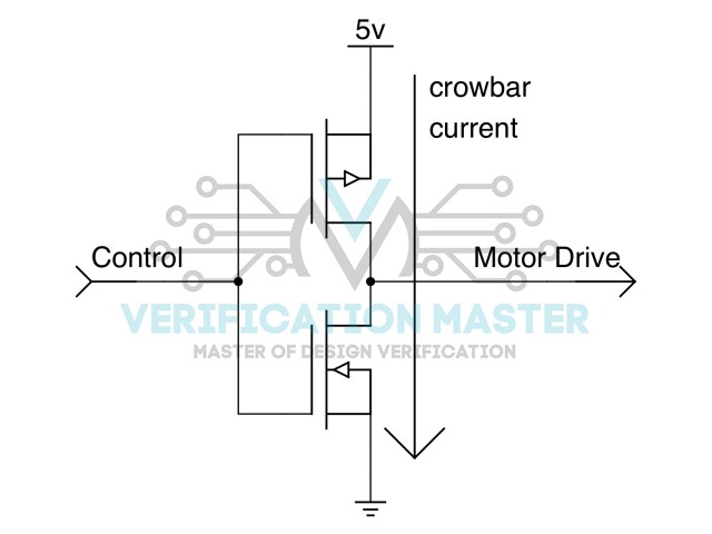
Short Circuit Power/Crowbar Current
There will be a situation where PMOS and NMOS transition comes to a threshold level. At this point, both PMOS and NMOS are shorted by creating a rail from VDD to VSS.
This short circuit between VDD and VSS results in power loss which is called short circuit power. So the expression is
Short Circuit Power= VDD*Isc

Crowbar Current
Static Power/Leakage Power
This is due to unwanted subthreshold currents in a channel of the transistor when turned off. High VT/ Regular VT are less leaky when compared with Lower VT and Ultra-low VT. So block using of Lower VT Cells in design or reduce them to a maximum extent.Better make use of it below 15%.
Routable Design
Having less Net length and lower congested design makes it a good Routable Design.
How to run Congestion Map? (Follow these step when congestion is found while performing placement steps)
By default Global Congestion Report is generated.
Choose Route–>Select Global Route congestion in GUI.
Two ways of generation Congestion Map:
- By using track assignment.
- By using Detail Route in design.
By Using Track Assignment:
Choose Route–> Select Track Assign Congestion Map in GUI.
By Using Detail Route:
Choose Route–> Select Detail Route Congestion Map in GUI.
How to generate a Congestion Report?
icc_shell> report_congestion
By default Global Route Congestion Report is generated.
Generated congestion information is stored in the Milkyway database.
Congestion data is by default stored for each layer. This enables the tool to generate layer-based congestion.
If a layer-based congestion map is not required,
Set layer_based_congestion_map Zroute global route option to false.
Analyzing Congestion
Zoom into the congested area to see the overflow number on the global routing cell. For Example, the red highlight on the edge of the global routing(GR) cell shows 12/4.
This means there are 4 tracks available, but 12 tracks are needed.
Minimal/No Cell and Pin Density and Congestion Hotspots
Making sure there is a fewer number of pins and cells located in a particular place such that it avoids the congestion in design. When there are more pins/cells in a place it would lead to the requirement of more routing tracks and if this availability is less when compared to required it would result in congested design.
Minimal Timing DRV’s(Design Rule Violations)
Having lower timing DRV’s like max_cap(capacitance), max_fanout, max_trans (transition) so that they do not violate the timing of the design.
How to reduce congestion? (Follow these step when congestion is found while performing placement steps)
Placement Blockages
To avoid placement in some areas, placement blockages are used. Different types of placement blockages are Soft, Partial, and Hard Blockages.
Soft Blockages: It restricts the placement of standard Cells in the blockage area but allows buffers(Optimization Cells) to be placed at the time of optimization to meet timing.
Hard Blockages: It prevents cells from being placed in the blockage area. Both Standard Cells and Buffers are prohibited inside hard blockage areas.
Partial Blockages: Designers can customize the amount of space required for placing optimizing cells like buffers and Standard Cells inside the blockage area.
Cell Padding
This is applied to standard cells in design where there are hotspots in design when a congestion map is run to get congestion analysis after standard cell placement. This technique is reserving some space on the left and right side of standard cells. While reserving space these cells move apart a little reducing the congestion at a particular space which is the hotspot shown in the design. As the height factor is constant, top and below space attainment is avoided. Only on the right and left sides of a standard cell, the padding is performed.
Creating bounds can also help in solving congestion. This is explained in later stages.

