The floor plan is the first stage in the physical Design.
The floorplan is a critical and important step because your quality of the chip depends on how good the floorplan. A good floor plan can simplify the implementation process (place, clock tree synthesis, route) simple. On the other hand, a bad floor plan can create issues in the design like congestion, timing, IR drop, routing issues.
We define chip or block’s size and shape in floor planning, place the IO pins/pads, Marcos, and blockage in the core or chip area. Also, it creates wire tracks for the placement of standard cells.
Building a Floor plan is similar to building an apartment. Let us compare:
- Both built from the ground to up.
- The apartment has proper parking for cars, Floorplan has an IO pad
- The apartment has rooms, Floorplan has macros.
- The apartment has a staircase for connectivity, Floorplan has interconnect.
- In apartments all rooms have their functions, In Floorplan, all the modules have their own function.
Type of Design
Flat Design
The complete chip’s physical design is done as a single block. Usually done for a small design.
Hierarchical Design
In this, the design is divided into several sub-circuits or partitions. Each of their subcircuits is then designed independently, often by separate teams. This subcircuit is assembled to create the full chip, and one of their sub-circuit partitions is called a Block.
In hierarchical design big complex design(BlockA) is divided into small sub blocks(BlockA/1,BlockA/2,BlockA/3….) then the designers can work on the blocks separately. Once all the blocks are finished, they are integrated to create the final chip.
List of input files to the tool:
- Synthesis Netlist(.v):
- Contains the logical connectivity of cells.
- Timing library Files(.lib)
- Contains timing and functionality information of a standard cell and macros.
- Physical libraries(.LEF)
- Contains physical information of the standard cell, macros, pads.
- Technology file(.TF)
- Contain the number of metal layers and via.
- Synopsys Design Constraints(.sdc)
- It contains input and output delay of pins of each cell in the design and clock constraints.
Steps to perform Floor Planning
Sanity check before floor plan
- check_design
- check_library
- check_timing
Define width and height of core and die
Aspect ratio defines the size and shape of the chip. It defined as the ratio of width to height of the chip Ideally, the aspect ratio of design should be 1:1.
Aspect Ratio: width (horizontal routing) : height (vertical routing)
I/O placement/pin placement
I/O pins are placed at the boundary of the chip. Pin placement is an important in the floorplanning. Pin placement can be done based on timing, congestion and utilization of the chip.
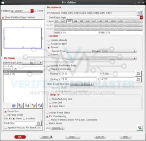
Steps to do pin placement in tool:
- Select pins
- Select edge (Top, Bottom, left, right)
- Select the layer (M1,M2…)
- Select the pattern for pin placement
- Put coordinates from where to start pin placement
- After we get this information, pin editor can be used to place pins.
- After pin placement to check that the pin placement is proper, we use command
checkPinAssignment
Placement of macros (Please refer to guidelines to place macros topic)
Adding placement and routing blockages as required (Please refer to blockages topic)
Adding tap cell and end cap cells (Please refer to different types of special cell’s topic)
Creating power mesh (Please refer to power planning topic)
List of Output file as a result of Floor Plan Steps
- Database with floor plan.
- Marco placed a database.
- Standard cell placement area
- Floor plan Def (It contains die/core area, placed macros information, blockages information, placed IO pin/ pad information.